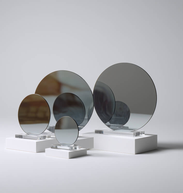
We collaborate to unlock new possibilities, not just deliver wafers.
OUR APPROACH
01

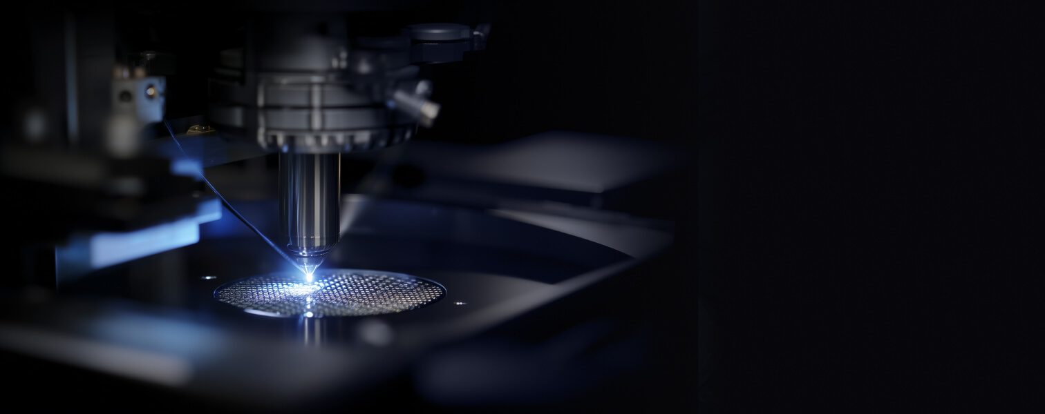
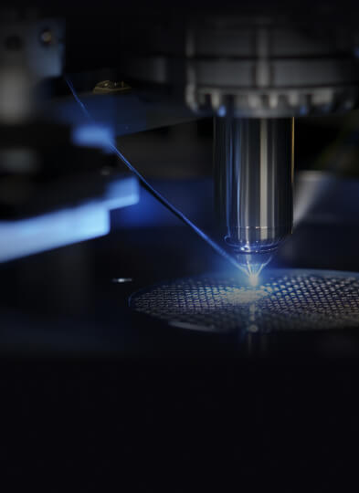
Chart the unseen
CREATE TOMORROW TODAY
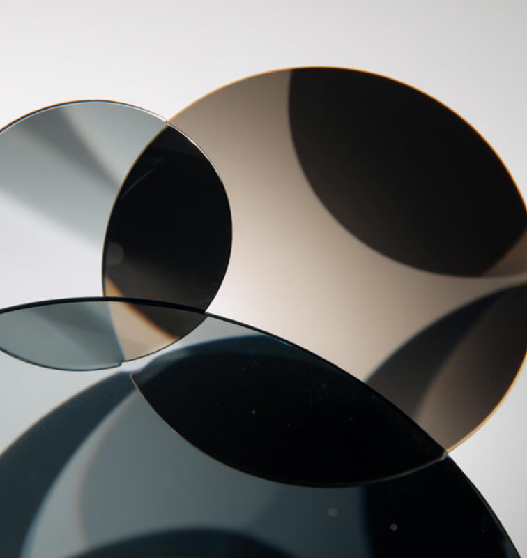
We don't optimize existing processes—we eliminate them. Our laser technology unlocks capabilities that conventional methods can't achieve, enabling previously impossible wafer geometries and specifications.
02

Light your path forward
PARTNERSHIP WITHOUT COMPROMISE
We work together to optimize wafer characteristics for your applications. From discovery to delivery, every specification serves your end goals.
03

Create a halo effect
CLEAN INNOVATION THAT PERFORMS
90% waste reduction and superior yield create benefits that ripple through your entire operation—better wafers, better devices, better outcomes.
Why it matters