Eliminate expensive tools while reducing labor costs through full automation
Enlightened
Engineering

Who we are
For industries driving tech forward, Halo is the most advanced laser-based manufacturing partner, unlocking the power of light for cleaner, smarter, more scalable production.
Performance
without capital
Performance
without capital
01 service
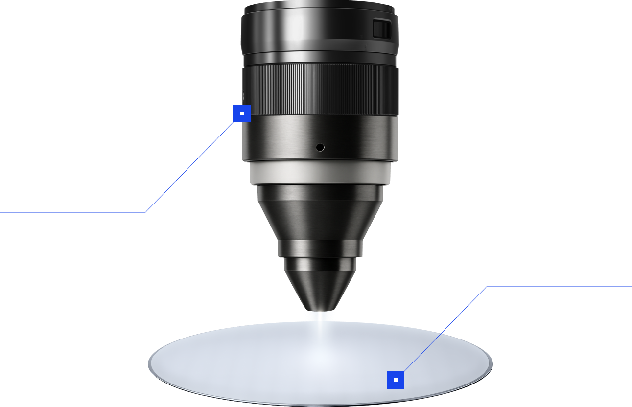
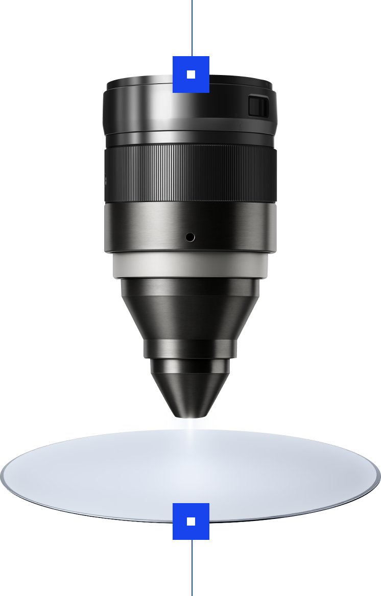
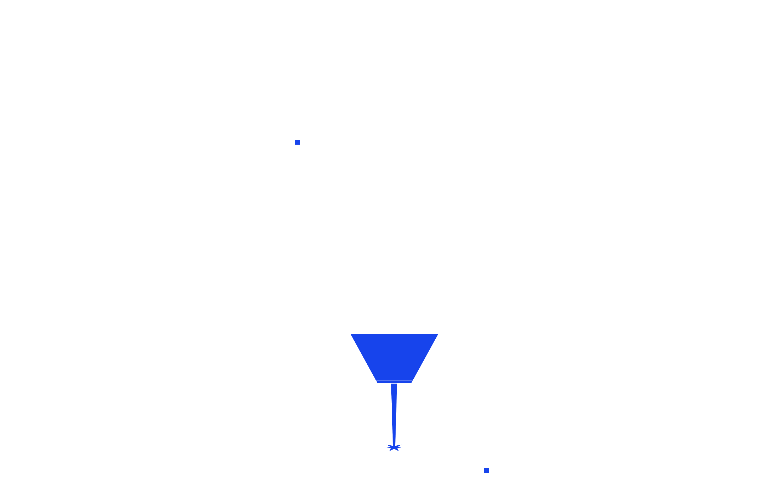
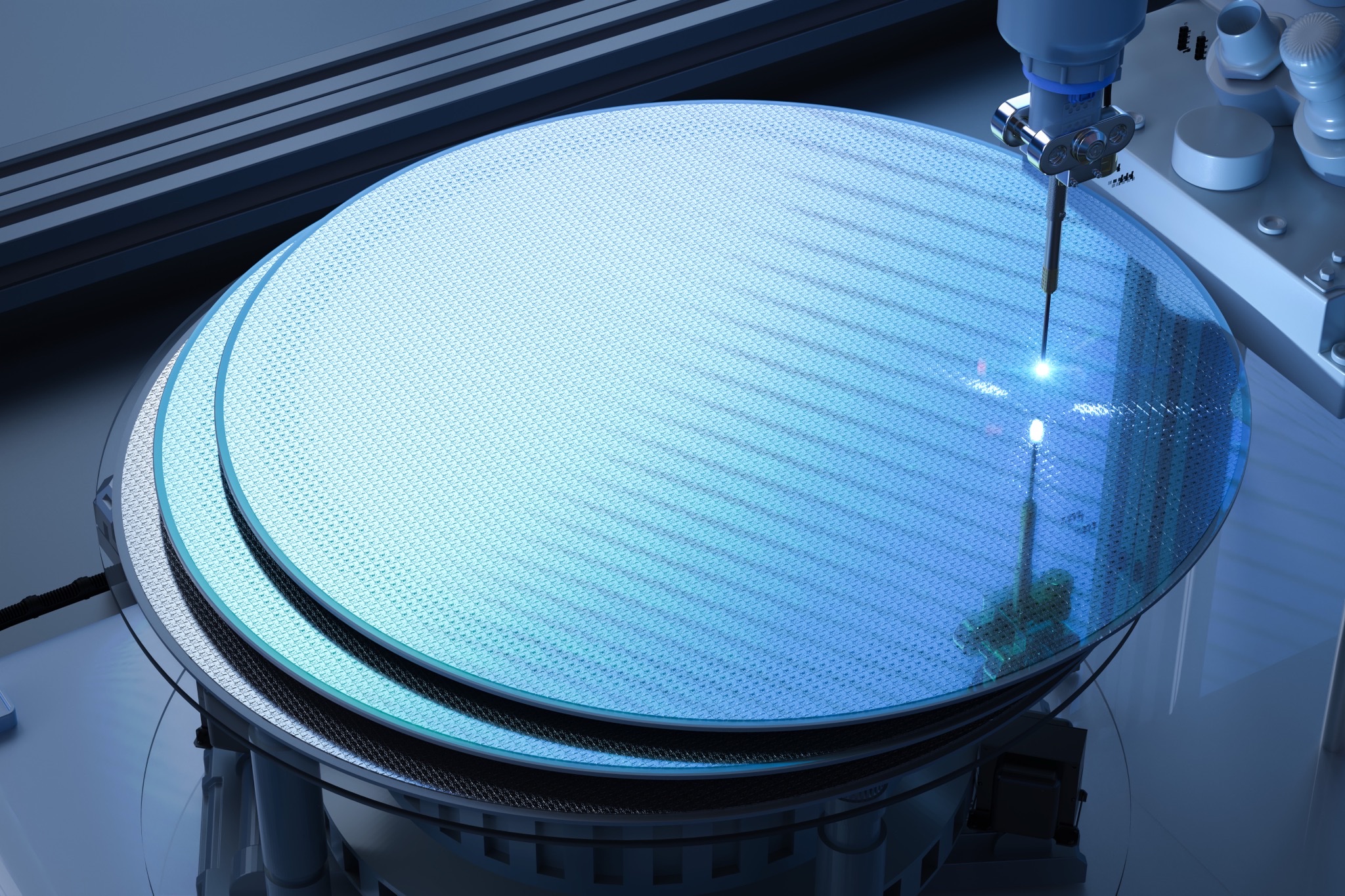
Laser wafering services
We deliver manufacturing excellence as a service—no equipment investment, just superior results.
02 service
SiC wafers
Production-grade wafers in multiple thicknesses—engineered to power tomorrow's breakthroughs.
Who we are
Partner with precision
Minimize cost
Reduce waste
Achieve 2.2-2.3 wafers per mm with 90% kerf loss reduction
Improve quality
Laser-controlled geometry creates ultra-smooth surfaces that enhance device performance
Increase yields
Consistent process prevents stress damage while delivering predictable output
About us
Built at Stanford, backed by visionaries

Stanford innovation
Academic rigor meets manufacturing execution

Industry leadership
Backed by VCs and energy agencies driving deep-tech innovation

Expert team
Decades of experience in laser physics and advanced materials
Companies that invest in us: