Engineering tomorrow with today's light
Our solutions
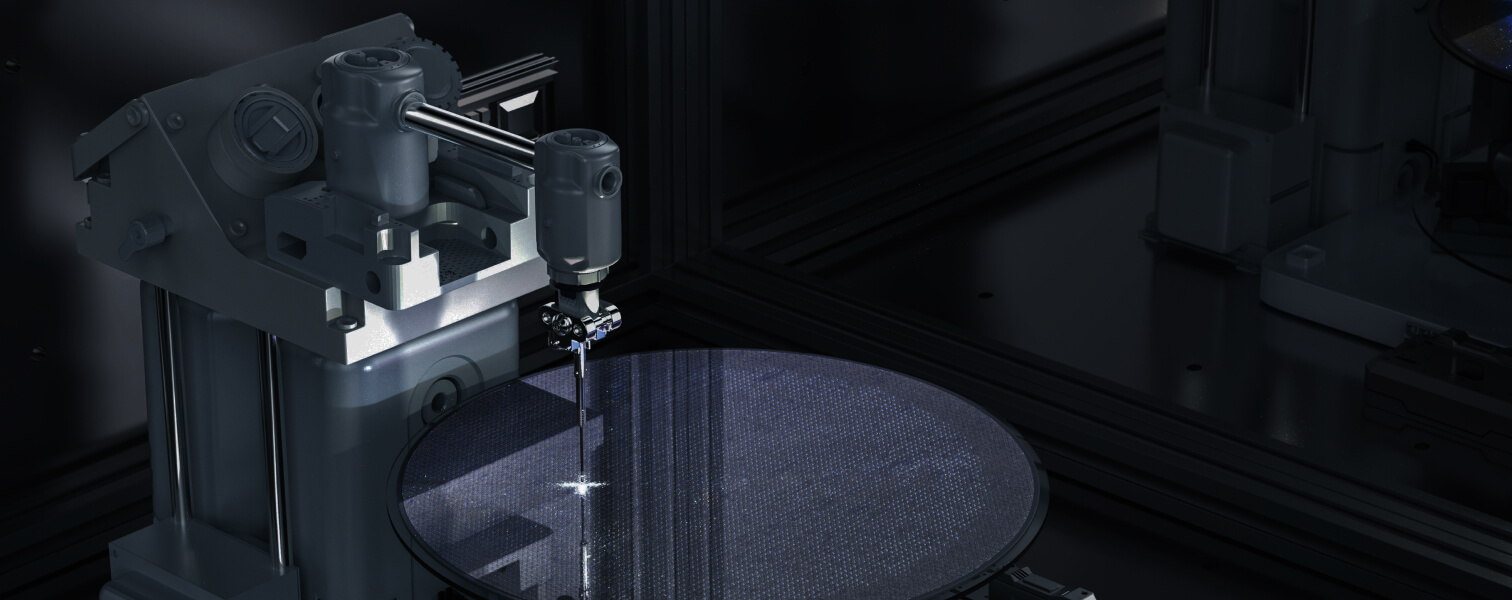
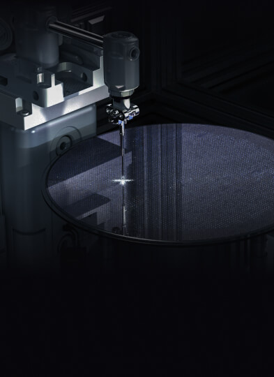
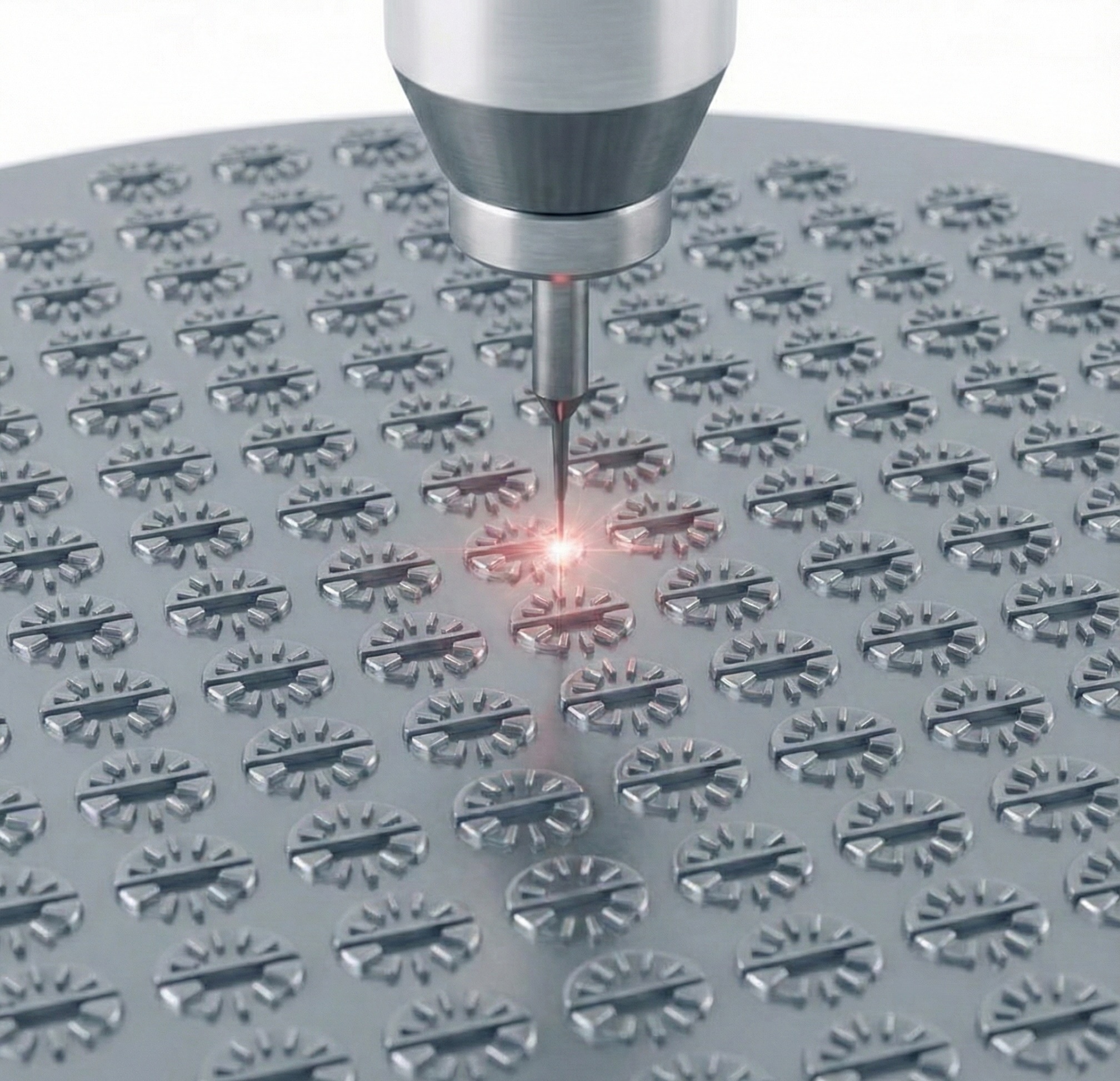
Harnessing the power of light to deliver precision, scalability, and sustainability across every stage of production.


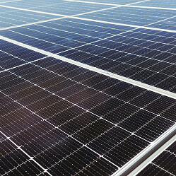
Powering progress
across industries


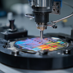

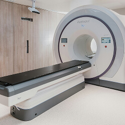

swipe right